 1")


Samsung applies EUV to 14nm DDR5 DRAM production
Last Updated on December 23, 2022 by Admin
[ad_1]
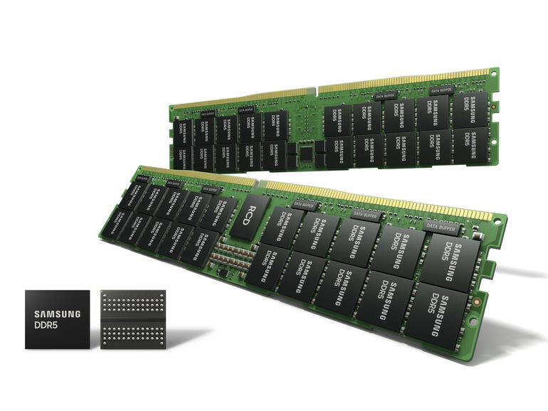
Samsung said on Tuesday it has begun mass production of 14nm DRAM, with extreme ultra-violet (EUV) lithography applied during its production.
The South Korean tech giant said it applied EUV to five layers of the DDR5 DRAM. This increased productivity per wafer by 20% compared to the previous generation, Samsung said. Power consumption per chip also improved approximately 20% compared to the prior iteration, it added.
Samsung said it would continue to apply EUV to more layers of DRAM 14nm and below to maintain its leadership in the memory chip market.
The South Korean tech giant, which is the world’s largest memory chipmaker, applied EUV to its DRAM production for the first time back in March 2020.
In March this year, it also introduced its first DDR5 DRAM module with 512GB capacity that was made with eight layers of 16GB chips.
For the latest 14nm DDR5 DRAM, Samsung said it would offer modules using 24GB chips.
At the same time, Samsung’s mobile business released a short video in a blog post on how it tests the Galaxy Z Fold 3 and Galaxy Z Flip 3. The clip shows the company’s various tests on the devices, which include an environmental chamber where the phones’ various features are turned on while going through different temperatures and climates.
In the video, the devices are also shown to be dunked in water, and folded and unfolded using machinery. For the Fold 3, other machines are used to draw lines on the device’s screen using the S Pen to ensure the feature is working.
RELATED COVERAGE
[ad_2]
Source link